(2014-06-05) Mechanical switches and snubber networks.
Current-ratings are typically for AC only (derate by a factor of 5 for DC).
We start our presentation of electronic circuit components with
a quick study of the lowly mechanical on/off switch
(called a "hard switch" as opposed to a
soft switch which merely powers down a circuit electronically,
without ever completely disconnecting it from its power supply).
This engineering challenge can be solved by a
snubber network which must be determined in
ways that are rarely properly discussed, if ever...
For ordinary 50 Hz or 60 Hz AC mains, the voltage becomes zero 100 or 120 times per second.
This helps break the spark which is created when an inductive load is switched off.
With DC, we have no such luck, as self-sustaining arcing is possible for high enough currents,
which could effectively prevent the circuit from being switched off.
To prevent this and/or reduce the long-term damage caused by sparks,
one simple idea would be to connect a capacitor (C) in parallel with
the switch. This would solve the arcing problem which occurs
when an inductive load is turned off but the new capacitor causes
a different problem when the switch is used
to turn the DC power supply (or "battery") back on...
In the off position the capacitor will typically see the entire voltage (U)
of the battery and could store a substantial amount of energy which
will be dissipated almost instantaneously into the switch when it's turned back on.
To solve this new problem, we may connect a resistor (R) in series with the capacitor C.
It will dissipate most of the aforementioned energy if its value is much greater
than the unavoidable contact resistance of the switch.
However, that resistor limits the effectiveness of the capacitor in addressing
the first issue raised.
Thus, there's a tradeoff which should be properly analyzed to
work out optimal values for R and C. Let's do so:
The above picture shows the situation just after the switch has been
turned off. The capacitor is discharged because it was previously
short-circuited by the switch. On the other hand, the current through
the load still has its previous value (I) because of the assumed inductive
properties of the load. The current I is now flowing through the
resistor and the voltage across the switch is therefore equal to RI,
which should not exceed the voltage rating for the switch (U0). So:
R < U0 /I
With the switch off, the capacitor gets charged to the full voltage of the
power supply through the connected load. When the switch is turned back on,
the capacitor discharges an initial current U/R through it.
That should not exceed the current rating of the switch (I0). So:
U/I0 < R
All told, we must have:
U/I0 < R < U0 /I
The above analysis is for transient regimes only.
When two switches are used in parallel (a DPST used as SPST) one
of them may have to withstand the whole transient before the other comes into
play and the snubber network should be planned accordingly.
Let's use as an example the little DPDT slide switch sold by Radio-Schack
as 275-0033 (pack of two).
As that switch is rated 500 mA at
30 VDC, we may consider using both sides in parallel to switch a
power supply rated 1000 mA at 9 V.
As a single side may have to absorb all the transients, we should use
the above analysis with I = 1 A
and I0 = 0.5 A. So:
U/I0 = 18 W
< R < 30 W
= U0 /I
Thus, we may want to choose for R a standard value of 22 W.
The above consideration are useful to obtain a rough figure.
However, they are based on a dubious type of "rating":
Switches are not rated in terms of the maximum voltage or current a switch can withstand.
Instead, a given switch can be given several such ratings, where
the power obtained as the product of those two quantities
is a constant (e.g., the same switch can be rated for 3A at 120VAC or 1.5A at 240VAC
to express a power rating of 360 VA).
The value we should use for C is derived from timing considerations
which may or may not be predictable. Some switches feature
a spring-loaded mechanism which makes the switching time short and predictable.
Other switches are typically slower and less predictable
(the timing characteristics of slide switches depend very much on who operates them).
(2014-04-20) Operational Amplifiers ("Op-amps")
An easy component to use, for beginners and seasoned engineers alike.
Microcontrollers are primarily concerned with interfacing with our analog world.
No discussion of microcontrollers would be complete without a discussion of the analog circuitry
that can achieve that.
One of the easiest analog building block to work with is the operational amplifier
("op-amp" to the initiated)...
An ideal operational amplifier is a circuit powered by a DC source and
endowed with one poutput pin and two input pins (an inverting input and a noninverting input).
The voltage at the output is a very large multiple of the difference in voltage between the inputs.
That multiple (the so-called gain of the amplifier is so large, in fact,
that the feedback of such an amplifier, within a properly designed circuit,
will reduce to virtually zero the voltage difference between its two inputs.
Ideally, the voltage between the inputs is zero as is the current flowing from
one to the other. On the other hand, the current and the voltage delivered by the
output can both be anything the circuit requires.
Elsewhere on this site, I present an elegant way to introduce
the functionality of an operational amplifier as a combination of two strange dipoles:
One (called nullator)
imposes the value of both the current and the voltage between its pins
(making them both zero) while the other (called norator)
imposes neither. The combination of both is called a nullor :
A modern operational amplifier will provide a good approximation of this ideal behavior
with a few flaws that can be partially corrected only at a substantial cost.
For general applications, though, even the cheap ones are extremely good.
Let's present a few of the more common ones:
Dual-Opamp ICs :
The TL072 was introduced as a low-noise version of the extremely popular TL082.
Nowadays, it seems that only one version is produced (the low-noise one)
with different identification stamps for commercial reasons only.
However, if you get an IC stamped "TL082", you have no guarantee that it will be a low-noise version,
since it may have been manufactured before that practice came about or before the TL072 even existed.
For most applications, that makes little or no difference, though.
Characteristics of the most popular operational amplifiers
The standard pinout is that of the LM324,
which packs four operational amplifiers in a single 14-pin package;
3 pins per amplifier and 2 pins for the power supply.
Trimmable Single Opamps :
The standard pinout for single op-amps is that of the most common
LM741
which includes two pins (1 and 5) for connection of an optional 10k external trimmer
(the midpoint of the trimmer goes to the negative rail.
The trimming is performed by wiring the inputs together and attempting to
make an adjustement which does not make the output go to saturation
(or, rather, find a point close to where saturation swiches polarity).
Single-amplifier versions of the above dual op-amp packages are drop-in replacements for the LM741 but
the balance pins aren't connected at all (the internally-trimmed
value of the input offset cannot be ajusted externally).
One JFET op-amp whose offset can be trimmed externally like the LM741 is the
LF411.
The LM709
can be frequency-compensated with external cirduitry using pin 1 (balance input) and pin 5 (balance output).
A 14-pin version of the LM709 exists which is pin compatible with (obsolete) first-generation
operational amplifiers, which had to be stabilized with external components.
Video :Genesis of the transistor,
Bell Labs (1965) with modern introduction by George Kupczak (2012).
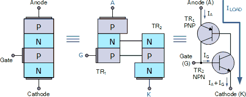
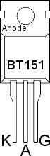
(2016-09-14) Thyristor (GE's Silicon-Controlled Rectifier, July 1957)
An SCR is a high-current bistable switch made from 4 layers of silicon.
A thyristor is rigorously equivalent to two transistors of
opposite polarities in series. In a pinch, or for low-current experimentation purposes,
you can make thyristors this way, which behave exactly like commercial ones.
(Diagram below courtesy of Electronics Tutorials.)
The above equivalence is also a good way to analyze the behavior of the thyristor.
When the gate (G) is brought to the potential of the cathode (K)
or below, the thyristor is nonconducting.
Conversely, when the gate is positive enough to allow some current from G to K,
the device becomes conductive and remains so without the need to maintain that current.
The above describes the standard P-gate,
or cathode-gated thyristor,
which is now synonymous with
SCR.
The less common N-gate polarity is dubbed
anode-gated thyristor
(AGT).
The AGT polarity is so rarely used that some practitioners aren't even familiar
with the corresponding symbol, shown at right (which is mandatory to properly describe triacs).
The previous schematics apply, with the only change that the external gate
terminal is connected to the other intermediate electrode.
Some thyristors are commercially available which have external connections
to both internal gates.
Such a four-pin device is known as a thyristor tetrode or a
silicon controlled switch
(SCS).
Video
(ECG 239).
In the early days, the undisputed champion for the SCR at General Electric was
Frank W. "Bill" Gutzwiller
(c.1926-2011).
Gutzwiller himself gave credit for the device
to the development team at GE led by Gordon Hall.
The thyristor was never patented, because GE's Patent Attorney (Bob Mooney) felt the claim would have been
too expensive to defend in view of the
pioneering
work on "PNPN switches" at Bell Laboratories,
by John L. Moll (1921-2011) in Sept. 1956, and by
J.J. Ebers (1921-1959) in 1952.
The original idea was first formulated by the Nobelist
William Shockley (1910-1989) in 1950...
Thus, there's no inventor on record for the thyristor.
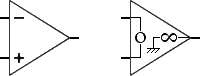
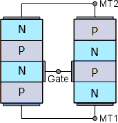
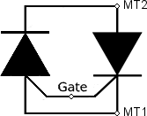
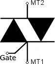
(2016-09-14) TRIAC (triode for alternating current, 1964)
A triggered triac lets current flow in one direction, until it vanishes...
A triac consists of two thyristors
of opposite polarities in reverse-parallel (i.e.,
the cathose of one is the anode of the other) sharing the same gate.
A triac is meant to conduct in either direction using whichever of its two consituent
thyristors is relevant.
The controlling voltage of the gate is
always understood to be with respect to the first main terminal
labeled MT1 (which is the cathode of the cathode-gated thyristor and the
anode of the anode-gated thyristor). The triac and its symbol are asymmetrical.
When used with AC a triggered triac will stop conducting
when the main current returns to zero.
To reduce the power (RMS)
delivered to a resistive load by an AC current, a triac in series is
typically retrigerred after some adjustable delay every time it stops conducting.
Because it acts like a switch (either on or off)
between its main terminals, the triac itself consumes little power and generates
little heat even when traversed by a fairly large current.
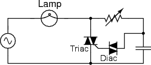
(2016-09-20) DIAC (diode for alternating current, 1964)
The standard way to correct assymmetric triggering on the gate of a triac.
A diac is a symmetrical device which starts conducting upon reaching its breakover voltage
(usually, 30 V or 40 V).
and remains conducting as long as the current doesn't fall below the holding current.
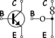
The simplest type of diac (e.g., DB3, discussed below) is just a low-current NPN transistor
without an external base connection and with emitter/collector symmetry.
As the voltage reaches the brakover voltage, enough current leaks
into the isolated base to force the transistor into the saturated state,
which it retains until current drops to zero again.
The device is engineered to withstand that regime repeatedly, unlike most ordinary transistors.
Most commonly, a diac is used in series with the gate of a triac
to make it trigger at a predictable fairly symmetric voltage (dissymetry less than 10%).
That configuration of a triac with a diac feeding its gate
greatly reduces the production of odd harmonics on the switched load.
It's commercially availaible as a single device, known as a quadrac.
The most common type of diac, by far, is the
DB3
bidirectional trigger diode (32 V nominal breakover voltage) which comes in a DO35 axial package
(usually dark blue) similar to a ¼ W carbon resistor.
Above is the schematics for the popular dimmer switch to power an incandescent lamp from
the mains (120 V or 240 V AC).
When the voltage becomes zero, the triac is off
and will start cinducting again when the voltage of the capacitor exceeds the diac's breakover voltage
(about 32 V).