For the more advanced part of the following review, a text file
is provided with the source code
for a tiny operating system and drivers for a parallel LCD unit and a synchronous serial
bus (I2C) connected to a real-time clock (RTC) with a temperature-controlled crystal oscillator (TCXO).
This example turns the unit into a bilingual clock/calendar with temperature display.
BASIC Stamp®
& other microcontrollers by Parallax, Inc.
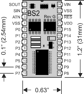
At left is the pinout of the bs2-ic 24-pin module devised by Parallax around a 28-pin surface-mount
PIC16C57C by Microchip.
16 digital I/O pins (P0 to P15) are individually accessible
in the PBASIC language designed for the BS2. They can also be accessed all at once via
a 16-bit register (INS/OUTS) or as one of two separate 8-bit buses,
or as one of four 4-bit ports.
Applications may also use a "virtual pin" (number 16)
for asynchronous serial communications through the port normally used for programming and debugging,
actually using the pins 1 and 2 on the BS2 board, marked SOUT for output
(cf. SEROUT)
and SIN for input
(cf. SERIN).
(2014-04-17) BASIC Stamp "HomeWork Board" USB
(#555-28188)
A review of an inexpensive microcontroller starter set.
At $40, this evaluation kit (also available at your local
Radio-Shack store) is $10 less expensive than
the bs2-ic Module
built into it, even though it includes a $4
USB A to Mini B Cable
and a little solderless breadboard,
(and ten 22-gauge jumper wires, for good measure).
Other Similar Parallax Products :
The downside is that the "HomeWork Board" can't be used to program an
actual BS2 for permanent installation in a less bulky standalone project.
To do that, you'd need a
28803 board
which goes for $99 and includes a bs2-ic in a socket
(to program several microcontrollers repeatedly, it might be wise to invest in a
24-pin ZIF socket
for "zero insertion force"). Otherwise, the 28803 and the board
we're reviewing here are equally suited as starter sets.
There are legacy serial versions of both units, which we'll ignore here.
Also, if you want to start directly with a better Parallax module from the table below,
you'll have to purchase it separately, provide your own 22-gauge jumper wires ($1)
buy a USB cable ($4) and get the same
carrier-board with no module on it ($70).
This would add up to more than $130, plus shipping.
Listed in the "speed" column is
the typical number of PBASIC instructions executed per second.
Like an older BS1 module
(and/or the low-cost BS1 evaluation board)
a stand-alone BS2 would only need a
6 V to 12 V DC power supply.
The other units require 6 V to 7.5 V DC.
Opening the box and getting started :
The 555-28188 comes with four stick-on rubber feet to be placed next to the corner holes
(which are meant for stand-off screw posts, if you decide to put the board in a protective
enclosure later).
The instructions are silk-screened on the board's flipside. They read:
Before you connect your board:
1. Install free software:
http://www.parallax.com/basicstampsoftware 2. In the software, click
Help > BASIC Stamp Help...
3. Follow the Getting Started steps.
Find Stamps in Class activities for the genuine
BASIC Stamp 2 that is built into this board:
www.parallax.com/education
You should only connect the board to your computer
(using the USB cable provided) after installing the Parallax
software on the computer and putting in a fresh 9V battery (not included).
The installation puts a "Basic Stamp Editor v2.5.3" (or possibly some other version number)
on the run menu but not on your desktop (copy the icon from the start menu to
your desktop and/or taskbar if you so desire).
The first time you run that software, it asks you if you want to associate the
related file types to it (.bs1 .bs2 .bse .bsx .bsp .bpe .bpx).
Allowing it to do so will simplify your life
(those file types are not of any use outside the Basic Stamp world, anyway).
At startup, you're shown one of 36 "tips of the day".
The first of these doesn't apply to USB boards but it mentions incidentally
that there's an online manual. I quote:
Use a standard straight-through serial cable to program the BASIC Stamp.
A null-modem will not work. If you're careful, you can make your own cable...
just follow the wiring diagram in the
BASIC Stamp Manual v2.0.
Following the instructions on the backside of the board,
we click the Help menu and choose the first item in it
("BASIC Stamp Help..."). Then, we click "Getting Started" on the left-hand column.
The first task is to identify your board.
The board reviewed here corresponds to the fourth picture listed
(the last one in the v2.5.3 revision of the software). Just click
the "next" button corresponding to that picture
and perform the setup tasks described, starting with affixing the
rubber feet (in case you've resisted the temptation to do so earlier).
For the initial "Run/Identify test", you should wait a few seconds
after the USB cable is plugged-in for the first time ever
(this gives your computer a little bit of time
to install the proper drivers and flash the message "Device is now ready to use" when that's done).
It's useful to know that the F6 key can be used to perform the "Run/Identify test"
whenever the BS communication sofware is up and running.
Since the unit has no power switch, you must disconnect the battery to turn it off.
However, it's virtually impossible not
to discover that one of the contacts comes off more easily than the other,
so that you can just leave one side plugged-in and rotate the battery to switch the
unit on and off (albeit unreliably so).
I've seen at least one other person do that publicly, at the end of a
video-proof that people do have fun with this thing
(see Sorting M&Ms by color).
A more reliable low-cost solution, without defacing the board, is to
connect the battery vertically to only one contact
(I prefer the outside one, the negative ground)
and close the circuit with a battery snap connector cut in half,
with some switch soldered between its two leads.
Either that or use an unbutchered snap obtain a pair of wires
which can connected (with am on/off switch)
to any suitable DC power source (there's a nice low-drop LM2940L voltage
regulator on board, so voltage requirements for an outside power supply
shouldn't be too strict).
I decided to base my own solution on a 9V
power supply with an "M" plug (5.5 mm OD, 2.1 mm ID, positive center)
specifically marketed for Arduino microcontroller boards.
Since not all such units are created equal
(there are a few horror stories floating around) I decided
to proceed cautiously and ordered first from Amazon a
made-in-China unit
with great reviews, rated 9V 650 mA
(for $6.50 + $2.99 shipping).
Not only does this little switching power supply work as it should
but it has a very nice form factor which accomodates crowded power strips.
The Chinese manufacturers goes by the name of Super Power Supply®
and they ship online orders to the US market from an address in Indiana
(8748 E. 3rd Street, Indianapolis, IN 46226-6516).
I was so pleased with their product that I tried to order more from them.
As I couldn't find the cute little thing in their catalog, I settled
for the closest thing
(SKU 06-861) rated 9V and 1000mA, although the picture showed a lousy form factor.
I ordered two units which arrived in my Los Angeles mailbox 3 days later.
I was pleasantly surprised to discover that they were identical to the one I had,
in every respect except a 50% higher current rating on the label!
I paid $14.27 ($4.89 per unit plus $4.49 S&H).
By itself, the board draws about 9.1 mA (measured) at rest when powered
with a 9 V battery. The TL082 which we shall soon add as part of our
first "real" interface (converting digital PWM into a clean analog signal)
will draw an additional 2.5 mA at rest...
Wiring some Standard Interfaces
Before I even touched this unit or looked at the online documentation,
I had a few fun applications in mind for this initial review.
One of them was generating DTMF tones.
I was therefore shocked and amused to discover
that this idea is so common that one of the 42 commands in the PBASIC language
(DTMFOUT)
is dedicated to that and makes the software part trivial.
The command generates the tone digitally in PWM mode (pulse-width modulation)
since there's no digital-to-analog converter on board.
This can be directed to any any pin but I'll dedicate P1 to that usage
(for a trivial reason which shall be given soon) and put
a good active filter on it
(Parallax recommends a 2000 Hz cutoff frequency but I'll use 3300 Hz to
allow a larger range of audio tones, beyond TouchTone®).
It's always a good idea to give several nonconflicting functions to the same I/O pin,
especially for decision intended to be permanent
(we don't want to waste pins, as we only have 16 to play with).
So, I'll also attach a bicolor diode to P1
(RadioShack #276-0012) which will be yellow
(= red+green) when there's audio activity, red in a 0 state, green in a 1 state
and unlit in the high-impedance state.
The bicolor diode consists of a red LED and a green LED mounted in parallel
with opposite polarities in a single package with two pins
(marked like the green LED would be if it was by itself).
One way to achieve that functionality would be to
connect the bicolor LED between P1 and a point connected to both supply rails
by the proper current limiting resistors
(equal values of 1k or so work fine because the two
diodes have similar voltage drops of 2.0 V and 2.1 V).
It works fine by presents one design flaw: A current of several milliamperes
will drain the battery even when the unit goes into sleep mode
(where only microamperes are darwn).
A better solution is to connect the bicolor LED between P1 and something
whose polarity is opposite to that of P1 when P1 isn't in the high-impedance
state. So, we'll make sure that the first stage of our active filter
is simply an inverting amplifier in the DC regime (at 0 Hz)
so we can connect our bicolor LED (with a current-limiting resistor)
between P1 and the output of that stage. At first, we may be satisfied
with just one stage and a single capacitor.
(2014-04-22) Pulse-Width Modulation (PWM)
Converting a PWM digital signal into an analog signal.
It's certainly not necessary to have access to an oscilloscope to use the Stamp.
However, a few oscillosope screenshots will help illustrates the concepts we have to teach now.
Pulse width modulation (PWM) denotes any encoding of an analog level
by a digital two-level signal whose duty cycle is proportional to the amplitude of the analog level.
The method used in BasicStamps to convert an 8-bit input level is to add the corresponding 8-bit value
(between 0 and 255) to an 8-bit accumulator. The value of the carry bit generated by this
operation is what the binary output (0 or 1) will be for the duration of the current PWM
interval (a unit of time which, for the unit reviewed here, is equal to 3.8 microseconds
for all PWM-related commands except one, as discussed below).
The beauty of this scheme is its simplicity and the fact that it remains valid if the desired
analog level changes over time (just adjust the content of the accumulator
to reflect the level change). This is how the Stamp generates siwaves and dual tones.
Let's use an example to design, once and for all, a proper audio output for our microcontroller.
We shall be aiming for the same cutoff frequency as traditional telephone service,
namely 3400 Hz.
A simple first-order lowpass filter is used for the preliminary demonstration.
A 3400 Hz cutoff would be approximately achieved with
a 4.7 kW resistor and a 10 nF capacitor.
(or 47 kW and 1 nF).
Counting the 220 W built-in resistor on the output pin
and using the measured values of the components on hand for this demo, our first test was
actually conducted with a corner frequency of 3175 Hz.
1 / [ 2p
( 4680 W + 220 W )
(10.23 10-9 F) ] = 3175 Hz
The sawteeth in the blue "sinewaves" are part of
the signal at this point, as will be discussed in great detail shortly.
Note the differences in the amplitudes at 1000 Hz, 2000 Hz and 3000 Hz,
which are a side-effect of first-order filtering and will be all but eliminated with
high-order filters.
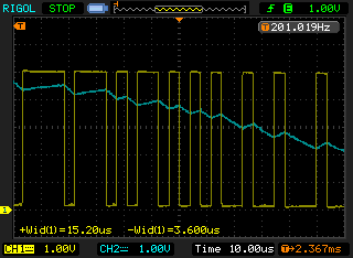
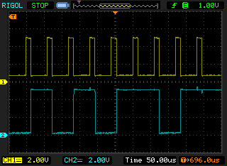
We dedicate a pin to properly trigger a Rigol DS1102E oscilloscope:
The signal displayed above on channel 1 (yellow)
is meant for the scope's "external trigger" input (using
a pair of clips attached to a BNC cable).
Note that the width of the pulse can be precisely measured to be 184.8 us
using a higher timebase resolution (that's a more precise value than the "180.0 us" in the
above screenshot at low resolution). That's an interesting measurement of the time it takes
to execute a very simple PBASIC step, which translates into 5400 steps per second
(the BS2 is advertised to execute 4000 "typical" PBASIC instructions per second).
The rising and falling edges of the trigger signal need not be adjacent.
Place them separately anywhere you like in your program to examine two different parts of the
main loop in more complicated cases, without the need to tax the scope's delayed timebase.
The two triggering options can then be selected on the scope without reprogramming the microcontroller
under test (although it takes only a few seconds to do so).
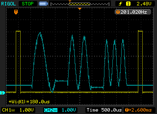
We now show details of the 2000 Hz "sinewave" burst
from the above test, along with the driving PWM digital signal (yellow trace).
Transitions can only appear at regular intervals of 3.8 us
This PWM cycle, used in the algorithm described above,
corresponds to 76 cycles of the BS2 clock, at the
advertised rate of 20 MHz.
In this screenshot, the scope shows the correct duration
(4 units = 15.2 us) of the first whole interval on the screen and
underestimates the second one by 5%
(it can find the correct value of 3.800 us using shorter time-scales).
This 3.8 us constant interval, corresponding to a PWM sampling
frequency of about 263.16 kHz, is the same
for all PWM waves produced by the BS2 firmware
(single frequency, double frequencies or touchtone).
Unexplicably, it's slightly longer (4.4 us)
for the PWM
command itself, which merely produces the PWM equivalent of a static level.
To make it easy on yourself,
one cost-effective way to go beyond the above first-order filter is to
use a commercial DSL filter, which is normally
designed to have the aforementioned corner frequency (around 3400 Hz).
Such filters are typically third-order or better...
(2014-05-18) Variable-Gain Amplifier (VGA) for a PWM Signal
The trick is to attenuate the PWM square wave before filtering it.
So far, we have decoded the PWM digital output from the microccontroller into a good
analog signal. The BasicStamp firmware could easily have encoded different
analog levels in its PWM tones. Unfortunately, it did not. So, we
have to find some hardware solution to the problem of allowing software to control
the audio volume.
The analog counterpart of what we are after is called a voltage-controlled
variable-gain amplifier. As a purely analog project, that would be a
fairly intricate endeavor, well beyond our current scope.
However, we can simplify things greatly by noticing that a PWM signal
can simply be used to chop up (turn on and off) some constant
DC level different from the whole supply voltage.
Filtering that square wave will result in a signal proportional to the DC level used.
The first step is to produce a steady analog voltage from a PWM signal on
some other pin. To do that we use the second high-impedance opamp
in the IC (TL082 or TL072) whose first half we've already used as an active filter.
Let's dedicate one pin (which we'll call LEVEL) to the audio gain control.
We connect LEVEL to the non-inverting input of the operational amplifier wired as
a voltage follower (i.e., the output is connected to the inverting input).
Let's now connect a 22 nF capacitor, say, to that pin
(and nothing else, not even a probe tip).
The charge on the capacitor has essentially nowhere to go when the microcontroller pin is
in its high-impedance state. So, we have a constant voltage at the output of the
operational amplifier which will take a very long time to decay...
Much more than what we need to maintain the output volume of every separate tone,
for a few seconds, at most.
With a metal-film capacitor of 22.8 nF on the breadboard,
I measured a time constant of 3528 s
(nearly one hour) which translates into a combined resistance of
155 GW for all pathes to ground in this casual test.
That would mean that the volume of a continuous tone would decrease at
a negligible rate of 0.0024 dB/s (3 dB after 20 minutes).
Note that we should not use the OUTPUT command for the LEVEL
pin. Doing so would force the state of the pin low or high for a substantial
amount of time (at least 184.4 us, remember?) and we don't need that;
the PWM command makes the pin an output pin only for the duration of its execution,
which is exactly what we want.
(2014-06-22) Using an alphanumeric LCD with a BASIC Stamp 2
With a BS2 (or equivalent) PBASIC offers no built-in LCD support.
As this is really a continuation of the previous educational introduction, using
the inexpensive HomeWork Board equivalent to a
Basic Stamp II (BS2)
we'll do more work to really get to the bottom of things.
Our reward for not cutting corners will be a couple of final answers
to software and hardware issues which are very often badly butchered...
For units beyond the BS2, Parallax provides 3 specific PBASIC commands which
facilitate 4-bit parallel interfacing with
an LCD (liquid crystal display) driven by the industry-standard
Hitachi HD44780character-LCD controller (namely,
LCDCMD,
LCDIN
and LCDOUT).
We'll discover that the scheme has one imperfection, in theory if not in practice
(a fourth specialized command should have been provided for the early steps of initialization,
accomplished in 8-bit mode with an irrelevant low-nibble).
The HD44780-compatible LCDs are commonly available in several formats:
We'll make our wiring compatible with one of the configurations supported by Parallax in the
aforementioned specialized LCD primitives.
Then, we'll discuss PBASIC software to support that configuration
and turn the whole thing into the educational experience it was meant to be.
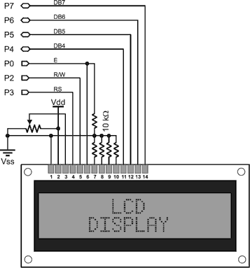
7 pins are normally used to interface with the LCD.
Some people use only 6 pins for one-way communications with an LCD (write-only)
by tying to ground the R/W pin (number 5 on the standard LCD connector).
I don't recommend that shortcut at all.
With the sole exception of the enable pin (number 6 on the LCD connector)
all pins are used only temporarily by the LCD and can be shared by other devices.
A priori, we had four choices for the HD44780A enable signal: (P0,P1,P8 or P9).
The rest of the wiring would have used pins 2-7 for the first two cases (enable on P0 or P1) and pins 10-15
in the other cases.
I'll use P9 here, which entails the use of P10 for R/W, P11 for RS and P12-P15 as data bus.
When the LCD display is not accessed, P12-P15 can be used as a 4-bit bus for other purposes,
keeping in mind that this bus is not put into a high-impedance state when the LCD is disabled
but features 30k pull-up resistors instead (as discussed below).
LCD units without backlighting have connectors with only 14 pins instead of .
Pin 15 is the anode (+) of the
backlight and pin 16 is the cathode (-).
Connect 16 to ground (Vss) and connect 16 to the positive 5V power rail
through a current-limiting resistor.
In the BS2, every I/O pins is protected by a resistor
of 270 ohms or so, which is great for a yellow-green LED backlight.
In my test unit, the back
(which such a protected pin will drive directly at 6.74 mA with a voltage drop of 3.15 V).
The potentiometer on pin 3 of the connector (often dubbed "contrast") is crucial.
It establishes the Vee voltage of the LCD, which should be ajusted according
to room temperature for best results.
If Vee is too low, off-pixels are visible. By increasing Vee, an optimal voltage is reached
where the off-pixels disappear, but barely so (increasing the voltage beyond this
would make the on-pixels fade away).
At this writing for example, room temperature is 28°C
(83°F is typical of Los Angeles in June)
and the optimal Vee for my test unit is 780 mV
(better described as -4.2 V with respect to the LCD anode).
Because the optimal "Vee" depends on temperature, it's somewhat unpredictable
and the user should be able to adjust it with a trimmer.
If the unit is meant to operate in various environments, an automatic compensation
for temperature and/or supply voltage could be considered (especially when using a
microcontroller with a spare analog voltage control).
Sometimes, the best voltage can be negative with
respect to the cathode as well (especially for 3.3 V circuits)
and a negative rail becomes indispensable for best results.
Different LCD Formats :
On a multi-line LCD character display, the positions of the characters in a given line are always
numbered consecutively from left to right.
What varies from one LCD to the next are the numbers assigned to the first character of each line.
The displays that feature 4 lines of 20 characters behave as if they consisted
of 2 lines of 40 characters.
whose second halves appear as the third and fourth lines of
the actual screen, which is filled by autoincrementing from 0 to 79 (and back to 0) as follows:
Sequential numbering of the 80 positions in an LCD of 4 lines of 20 characters
0
1
2
3
4
5
6
7
8
9
10
11
12
13
14
15
16
17
18
19
40
41
42
43
44
45
46
47
48
49
50
51
52
53
54
55
56
57
58
59
20
21
22
23
24
25
26
27
28
29
30
31
32
33
34
35
36
37
38
39
60
61
62
63
64
65
66
67
68
69
70
71
72
73
74
75
76
77
78
79
However, this is not the way direct-access indices are organized.
Instead, the beginnings of the two lines are respectively at addresses 0 and 64.
The two sets of forbidden entry points at the "end" of either line (40-63 and 104-127)
behave exactly like the valid beginning of the next line (64 and 0, respectively).
Both forbidden sets are skipped when the LCD is accessed sequentially, by autoincrementing.
4 by 20 LCD random-access addresses
(40-63 same as 64 ,
104-127 same as 0 )
0
1
2
3
4
5
6
7
8
9
10
11
12
13
14
15
16
17
18
19
64
65
66
67
68
69
70
71
72
73
74
75
76
77
78
79
80
81
82
83
20
21
22
23
24
25
26
27
28
29
30
31
32
33
34
35
36
37
38
39
84
85
86
87
88
89
90
91
92
93
94
95
96
97
98
99
100
101
102
103
At left is the standard 5x8 matrix font for the HD44780. It's sometimes called a 5x7
font because the bottom row is blank in all standard characters to leave room for an underscore cursor.
However, this need not be the case for custom characters, especially in applications
where the underscore cursor isn't used.
The HD44780 provides only 64 bytes of CGRAM (character generator RAM) for custom characters.
In this 5x8 format, that's enough for 8 custom characters (each 5-bit row uses a byte)
encoded from 0 to 7 at the highlighted positions in the table.
In the rare 5x11 format (not covered here) those 64 bytes would only allow 5 custom characters,
numbered from 0 to 4, with 9 leftover bytes.
Like DDRAM (data display RAM) the 64 locations of CGRAM are accessible by address and successive
writes will cause an autoincrement to allow access to the next location.
Also like DDRAM, this autoincrement wraps around to the beginning of the available space.
If you must know, so do the codes of the custom characters.
(In practice, this means that the characters you defined for codes 0,1,2...
will also be available at 8,9,10...)
A dot indicates an irrelevant bit ("don't care"). Bit-letters are explained below.
In the last column are execution times (microseconds) for a 250 kHz clock rate.
Name
RS
RW
Data Bus
Instruction (action to perform)
ms
clear
0
0
0000 0001
Clear every display byte, reset cursor.
1640
home
0
0
0000 001.
Reset display shift, reset cursor.
1640
entry
0
0
0000 01as
Autoincrement (a=1). Allow shift (s=1).
40
show
0
0
0000 1dub
Display (d), underscore (u), blinker (b).
40
move
0
0
0001 cm..
Cursor (c=0) or display. Left (m=0) or right.
40
set
0
0
001w nf..
4-bit (w=0). Single line (n=0). 5x8 dots (f=0).
40
cgram
0
0
01,address
6-bit address in character-generator space.
40
ddram
0
0
1, address
Set 7-bit address in data-display space.
40
busy
0
1
BF,address
Fetch current address ("busy flag" in MSBit).
0
write
1
0
data
Write 8-bit data to current address.
40
read
1
1
data
Read 8-bit data from current address.
40
a (autoincrement flag) pertains to DDRAM access only. a=1 is the normal mode whereby successive
accesses correspond to indices in increasing order. To go backwards, use autodecrement mode (a=0).
The HD44780 data bus has pull-up resistors :
Let's nvestigate the high-speed protocol which avoids undue
delays for a fast microntroller (this doesn't apply to the BS2 running PBASIC, with a
single exception which is easily disposed of).
In the process of this investigation, I discovered that
the LCD's enable pin (pin 6 on the LCD connector, often called
"E" and dubbed LCD in the source code provided here)
doesn't put the LCD data bus in a high-impedance state, as expected.
Instead, the data lines sport 30k pull-up resistors,
which the designer should keep in mind when sharing this bus with other devices.
Once the LCD has been properly initialized, we may attempt to time the longest LCD
instruction to see if any extra delays are needed on the BS2.
The following BS2 program fragment is meant to visualize on the oscilloscope what
time is leftover in the worst case...
DO             ' Testing BF = Db7 with an oscilloscope :
char = LCDclr  ' %00000001 (Clear LCD) is the SLOWEST command
GOSUB LCDctrl  ' Send command (and leave RS low)
DIRD = %0000   ' Use 4-bit bus D as input (pins 12,13,14,15)
HIGH rw        ' This rising edge of RW will trigger the scope
HIGH lcd       ' Enable LCD
PAUSE 1        ' Monitor Db7 = BF with a 10k pull-down resistor
LOW lcd        ' Test complete, disable LCD
LOW rw         ' Back to write mode
LOOP           ' Repeat (more than 200 times per second)
The highlighted part of that program corresponds to the oscilogram below
(the yellow trace is R/W).
The 10 kW external pull-down resistor on BF
reveals the presence of the aforementioned 30k internal pull-up resistor.
The oscillogram below shows how
an LCD unit driven by an HD44780 makes a weak attempt to control the data bus
through internal 30k resistors (fighting an external 10k pull-down
resistor installed for the purpose) even when the LCD unit is disables!
The 30k value itself can be deduced from the screenshot at left,
where a 25% level is observed on Db7 = BF (blue trace)
as the pull-up resistor fights the external 10k pull-down resistor
(temporarily installed for this test only).
Likewise, the failure of the BF signal from the LCD to reach the 100% logic level
(which doesn't exist without the pull-down resistor)
can be attributed to an output impedance of 1.5k or so.
Some sloppy designers advocate grounding R/W under the dubious pretense of
"saving" a pin and/or a cable wire
(the latter at the cost of performing the grounding directly on the LCD connector).
If reading the LCD is permanently disabled by grounding R/W,
the LCD can't be used at full speed in machine language.
PBASIC, on the other hand, is so slow that the issue only arises
in the "clear-screen" command (used in the
above oscilloscope test). The "write-only" use in PBASIC
of an HD44780-driven LCD is thus totally safe if one simply waits an
additional 2 milliseconds after clearing the screen.
That's all there is to it...
With a microcontroller programmed in assembly language however, it's more satisfying
to drive the LCD in the proper high-speed manner
(reading BF before writing to the LCD).
When the microcontroller is in sleep mode,
output pins are still driven but will go out for about 18 ms
every 2.304 s.
During those regular outages, spurious strobes could occur on the LCD's "enable" pin
if we didn't install a pull-down resistor on that pin
(which is the only one permanently dedicated to the LCD unit, besides the backlight pin).
"Jitter" reveals the exact frequency of the LCD local clock:
Jitter is the phenomenon whereby events which could naively be expected
to happen repeatedly at a predictable time are actually observed to be randomly early or late,
within a definte interval of measurable width.
(In some contexts, that's also called phase noise.)
In the above, one can observe an obvious jitter on the falling edge of the BF signal
(blue trace). Its width can easily be measured to be about 17.6 us
(with the oscilloscope at 2us per division observe the jitter for several seconds,
placing one cursor on its lower limit and another on the upper one).
If we assume that the jitter is due to the
lack of synchronization of the BS2 clock and the microcontroller clock,
then the width of the jitter is equal to a whole number of cycles of the LCD clock
(presumably, the time it takes the HD44780 to execute each cycle of a waiting loop).
This means the clock of the tested LCD unit is a multiple of 56.8 kHz or so.
As the datasheet of the HD44780 specify a clock frequency between
190 kHz and 250 kHz, we may expect the clock frequency
of that particular unit to be about 227 kHz
and deduce that the HD44780 can't pinpoint the time of external
events to an accuracy better than 4 clock cycles, which seems reasonable...
(2014-04-19) Keypad with a BASIC Stamp
Giving birth to a standalone HW1 by cutting its USB umbilical cord.
Our goal now is to turn the HomeWork Board (HWB)
into a controlling device which can be operated without its USB umbilical cord.
We're already halfway into this with the LCD provided above.
In this section, we'll complete the process by endowing the unit with a 16-key keypad.
After this, the resulting standalone device deserves an enclosure and a name: HW1.
I'll install an off-the-shelf 16-key keyboard (the usual telephone keys plus an
ABCD column corresponding to the four extra standard touchtones).
The supporting software will recognize 136 possible input combinations from this:
16 single keys and 120 combinations of two keys pressed simultaneously.
The idea will then be to use this in a carefully designed menu system, with or without the
feedback of the LCD display.
(2014-05-23) Cheap Sonar Sensor
Bouncing ultrasound (40 kHz) off an object to measure its distance.
The HC-SR04 is a 4-pin device. Besides the power rails (labeled Vcc and GND)
there's an input pin labeled TRIG and an outpout pin labeled ECHO.
The device consists of a microcontroller driving two identical acoustic transducers
working at a nominal frequency of 40 kHz (ultrasound).
It sends an 8-cycle sound burst and measures the time it takes to receive the echo.
The unit is activated by a positive pulse on the TRIG pin
and responds with a positive pulse on the ECHO pin after a fixed amount of
time (on my unit, the leading edge of ECHO comes 466 us after the falling edge of TRIG).
The width of that pulse is the time it took to receive an echo
(i.e., twice the distance between the sensor and the object, divided by the speed of sound).
The duration of the trigger pulse is irrelevant as long as it exceeds the minimum specified
by the manufacturer, namely, 10 us
(although the test unit seems to trigger reliably on pulses as short as 5 or 6 us).
This demo lights up an LED when the measured distance is 204 mm or less:
' {$STAMP BS2}
' {$PBASIC 2.5}

trig  PIN 1
echo  PIN 2
led   PIN 3

time  VAR Word

LOW   trig        ' Equivalent to  OUTPUT trig : trig=0
INPUT echo
LOW   led

DO
PULSOUT trig,25     ' 50 us on a BS2 (10 us on a BS2sx)
PULSIN echo,1,time  ' Receive pulse width

IF time <= 300 THEN                 ' 204 mm at 340 m/s
  led=1 : ELSE : led=0 : ENDIF
LOOP
Clearly, the unit could have been designed to combine the output and input functions on a single pin.
Such single-pin devices are indeed available but they happen to be much more expensive
than the unit reviewed here...
(2014-04-22) Synchronous Serial Communications
Example: Real-time clock (RTC) using the I2C bus.
Our introduction to the I2C protocol will be based on a unit which contains
two independent I2C nodes; a real-time clock and a mid-sized EEPROM (4096 bytes of non-volatile memory).
The tiny board at left retails
below $6
(with shipping). It's built around a
DS3231 with an
integrated temperature-compensated crystal oscillator (TCXO).
On the "32K" pin is the output of the 32768 Hz oscillator
(300 ns rise time, 32% duty, 15 ns fall).
The programmable SQW output pin can deliver
a 1 Hz signal (300 ns rise, 20 ns fall, 50%).
Straight out of the box, without using its digital trimming capabilities,
the DS3231 has a 2 ppm accuracy
(between 0°C and 40°C) which translates into
1.2 s per week, or 1 minute per year.
To measure the accuracy of the clock in just a few minutes,
you may use the stable 1 Hz signal (often termed PPS for "pulse per second")
from a GPS receiver.
Use that signal to trigger a digital oscilloscope and observe the 32768 Hz
output with the timebase set at 2 us per division (so you can always
see several wavefronts on the screen). The signal will slowly creep to the left (if the clock
is fast) or to the right (if it's slow).
Measure the time T be the time it takes for the trace to drift on the screen by a distance
corresponding to a given interval (one microsecond, say).
The relative accuracy of the clock is simply t/T.
For example, with the factory settings ("aging register" set to zero)
I found that the trace was drifting to the left on the screen by
2.5 us in 36.32 seconds at a temperature of
31¼°C (according to the chip, but probably more like 29°8)
so that clock is too fast by the following relative amount:
(2.5 us) / (36 s) = 0.07 ppm = 2 seconds per year
A few minutes later, at the same temperature, it took only 26 seconds
for the same drift (that's 1 ppm). Then the drift seemed to stop when the
temperature (as measured by the chip itself) dropped only a quarter of a degree...
The data sheet says that the oscillator can be trimmed in steps of roughly 0.1 ppm
(the user-supplied correction is stored in register $10 termed
"aging register" and is updated every 64 seconds or upon request).
If found the influence of the aging register, if any, to be far less than that in the
conditions described above.
It looks as though the chip is significantly more precise than what's described in the
datasheet, but less adjustable...
My first impression about the unit test is that its untrimmed performance is
at the best level that digital trimming would permit,
according to the datasheet.
The influence of digital trimming, if any, is certainly far below the
0.1 ppm per step quoted in the datasheet.
My observations are thus consistent with the fact that the unit I am looking at
was trimmed at the factory to the best precision the hardware would allow
(roughly 0.1 ppm) with user-adjustable trimming now turned off.
The venerable DS1307
doesn't begin to approach that level of performance of the DS3231.
(In typical applications, the DS1307 relies on an uncompensated external 32768 Hz crystal.)
Besides the real-time clock itself, the above DS3231 board
(like its DS1307-based predecessors) includes an independent
32 kbit EEPROM
(4096 bytes of non-volatile data) which could be another good didactic I2C example,
albeit a duller one...
Before I got may hands on the part,
my intention was to use that EEPROM to store aging data on it
(the variation of optimal digital trimming over the years).
Because of the above considerations, this is now moot.
One nice feature of the DS1307 is that is has static RAM (SRAM) maintained by the clock battery
on the portion of the 8-bit address space not used by the actual RTC registers.
The DS3231 doesn't have that, but there is an otherwise identical IC
(the DS3232) which does.
Unlike the DS1307, the DS3231/DS3232 features a century toggle (located at
the most significant position of the month-number byte).
This is toggled whenever the century changes, to deal with potential bugs
at the beginnings of the years 2100, 2200, etc.
(Remember the Y2K millennium bug?)
To be able to properly determine leap years, a chip like that would need
to keep track of the century modulo 4.
That's only two bits, but the DS3231 doesn't have them.
Instead, the DS3231 uses the Julian rule
(which call for every year divisible by 4 to be a leap year)
and ignores the Gregorian modification to that rule used in our modern calendar
(where years divisible by 100 aren't leap years unless they are also divisible by 400).
The DS3231 will therefore fail on the first day of March in 2100, 2200, 2300, 2500...
The first bad day for the DS3231 comes only 59 days after the DS1307 will fail
for lack of a "century toggle".
However, a microcontroller using the DS3231 can still read the correct date from it
essentially forever
if it's only allowed to read the clock at least once per century!
I am ignoring practical details such as battery life and EEPROM data retention period
in this intellectual exercise...
To do so, we simply compare the day of the week maintained by the DS3231 (flawlessly)
to what can be computed from the date
(including the upper digits of the year, which the microntroller can keep update
for itself by reading the century toggle bit, if allowed to do so at least once per century).
Any discrepancy is settled by adding to the date a number of days (from 0 to 6)
equal to the difference between the computed weekday and the weekday stored on the chip
(the latter should never be adjusted).
This effectively cancels erroneous leap days (Feb. 29)
which the DS3231 would wrongly insert on three of every four century years
(2100, 2200, 2300, 2500, etc.).
This algorithm allows the correct date to be determined without ambiguity
modulo a period of 400 consecutive years
(one Gregorian period).
If the above algorithm is always executed before the time/date is displayed,
there isn't even a need to update the information stored on the chip
(but it's prudent to so, of course).
If you don't expect to be around in March 2100, you may safely ignore all of the above
but you shouldn't...
The I2C (Inter IC) Bus
The oscillogram below shows the transfer of a $56 byte
(standing for the value 56 in BCD) from a "slave" IC
(a DS3231 real-time clock) to a Basic Stamp 2 "master" (BS2) over an I2C bus.
Nine clock pulses are sent on the SCL line (yellow) by
the BS2 executing a fast-paced command:
SHIFTIN sda, scl, MSBPRE, [frame\9]
Normally, the BS2 should be listening for the first 8 bits and
pulling SDA low to ask for more data.
However, this is the last byte of a transfer
and the master must send a "1" bit (a NACK signal)
which is exactly like pretending to listen for a ninth bit!
This is part of a clock program where we only need to fetch a single bit
(the parity of the least significant digit in the count of seconds)
to check as fast as possible whether an update is needed,
so any trick goes...
Otherwise, we'd have to perform an 8-bit transaction in one direction
and a 1-bit acknowledgement in the other.
The slave changes the state of the data line (SDA) in blue, just after
each clock pulse.
Not visible at this time-scale is a reaction
lag of about 350 ns from the RTC chip and a
rise time (10-90%) of 165 ns
with a 2.15 kW pull-up resistor on SDA
(designed for 400 kHz "Fm mode" use).
As examplified above,
the BS2 can be used to communicate over an I2C bus as a master
(not as a slave, which is a much more demanding task).
The basic pace of the above example cannot be adjusted on the BS2 platform
(take it or leave it).
The basic BS2 clock rate for IC2 communications is 16.6 kHz
The width of each clock pulse is 14.24 us and the interval
between them is 46 us.
Almost all I2C devices are rated for at least 100 kHz and will
very easily accomodate the above pace.
Note that the BS2 uses push-pull on both bus lines in the relevant primitive,
instead of the open-collector architecture I2C is based on.
Models beyond the BS2 feature PBASIC primitives specifically designed for I2C (namely
I2CIN and
I2COUT)
but we are not reviewing those here.
This isn't much of a problem in practice, as long as the BS2 master never
pushes a hard "1" on a bus line (by contrast with a soft "1" produced by the
high-impedance "input" state) at times when the I2C protocol allows a slave to pull is low.
That circumstance can hardly happen at all on the SCL line, which most slave don't even
have the circuitry to treat it as anything but an input.
A few slaves may be able to "hold the clock" low to tell a fast master to wait during high-speed
transfers. This type of protocal is beyond the scope of this article.
When the master (the BS2) is speaking on the SDA line, all slaves are listening and it makes
very little difference whether the BS2 is using open-collector or push-pull logic
(the only difference on an oscilloscop is that rising times are faster, with a possible overshoot,
when push-pull is used).
Don't even think of allowing the BS2 to share an I2C bus with other masters or with
slaves that can "hold the clock".
On our side of things, it's essential never to let the BS2 attempt to write
anything but a zero at a time when it's supposed to be listening on the SDA line
(but doesn't care about the information). Or else a condition may result which is
technically a bad short circuit (no physical damage will result only because
of the BS2's built-in protection resistors on I/O pins).
In practice, this word of caution only applies to the writing counterpart of the 9-bit
read discussed above. The ninth bit in an I2C write is supposed to be written
by the slave (and it's normally low). If the BS2 chooses to overwrite
that bit, it better be a zero.
In other words, don't EVER use the following instruction unless you are absolutely
sure that "frame" is even!
SHIFTOUT sda, scl, MSBFIRST, [frame\9]
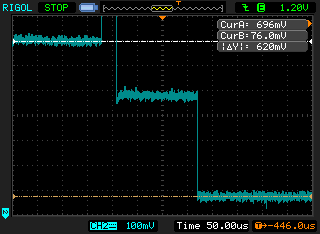
Below is a close-up view of the acknowledgment by a DS3231 chip of an I2C
request by a Basic Stamp 2.
Because its pin is protected by a substantial resistance, the BS2
can pull the SDA bus line only so low (696 mV)
against a 2.15 k pull-up resistor.
After the falling edge of the positive pulse on SDA, an intermediary level
(476 mV here, but it's sensitive to fidgeting with the breadboard)
is quickly reached which is maintained for a
surprisingly long time (165 us)
The I2C standard can achieve synchronous serial communications between many ICs
over a distance of a few meters, using only a single pair of shared lines
(besides the two power rails).
Every transfer over an I2C bus begins with a START signal (more about that later)
followed by a control byte containing a 7-bit code followed by a one-bit mode
(0=write, 1=read).
The 7-bit code can be one of 112 short slave addresses
or it can be one of the 16 commands tabulated next,
which ordinary (7-bit) I2C slave devices may safely ignore.
Four of these codes ($04-$07) are actually part of a rarely-used 10-bit addressing scheme,
which adds 1024 addresses (for a grand total of 1136 possible slave addresses).
This was introduced in 1992, as part of the first standardization of I2C
(launched by Philips 10 years earlier)
in anticipation of a yet-to-come crowding of the I2C space.
I'm not aware of a single commercial I2C chip with a 10-bit address but
I'm still providing full software support for it here (without slowing
down 7-bit operations by any significant amount).
Several 10-bit slaves may respond to a $04-$07 control code,
but at most one should acknowledge the accompanying extension byte.
Leading zeroes (in binary or hexadecimal) can be essential to avoid
confusion between long (10-bit) and short (7-bit) addresses.
$48 and $048 (%1001000 and %0001001000) are different.
Some misguided authors are ignoring the very real possibility of long (10-bit)
I2C addresses less than or equal to %0001111111.
There are no "reserved" 10-bit addresses; the 1024 possibilities are available.
Note that the designers of the I2C protocol saw it fit to specify that
the second part of a 10-bit address should only be given once at
the beginning of a combined transaction (read-write=read).
This improves the throughput of the bus a little but forces 10-bit slaves
to follow-up on transactions that partially match their address
in order not to mistake for their full address the combination of their own prefix
with some random data (which typically would happen 0.4% of the time).
7-bit Code
R/W
Meaning
000 0000
0
General call
000 0000
1
START byte
000 0001
-
CBUS format
000 0010
-
Other format (reserved)
000 0011
-
Reserved for future use
000 0011
-
Reserved for future use
000 0100
0
Hs mode master code test (0)
000 01xy
z
Hs mode master code xyz (1 to 7)
000 0011
-
Reserved for future use
111 10xy
R/W
10-bit address (xy bits & next byte)
111 1100
-
Device ID
111 1101
-
Reserved
111 1110
-
Reserved
111 1111
-
Reserved
Two I2C devices with the same address shouldn't coexist on the same bus.
The maximum capacitance allowed on each bus line (400 pF) restricts
the physical characteristics of the bus and the number of connected devices.
The original I2C bus was introduced by Philips in 1982 for a maximal clock rate
of 100 kHz (with a rarely-used slow mode limited to 10 kHz).
Unlike the earlier DS1307, the DS3231 chip reviewed here can also
operate in the so-called fast mode (Fm)
introduced in 1992, which allows clock speeds up to 400 kHz.
See below for recent upgrades.
The two I2C bus lines are called clock and data
and denoted by two standard 3-letter abbreviations:
SCL : Serial clock line.
SDA : Serial data line.
Both lines are open collector with pull-up resistors connected to the
positive power rail (that name assumes the lines are driven by
NPN transistors
with grounded emitters, but other equivalent technologies can be used
and the designation open drain is also common).
The logical state of either line is thus high by default and becomes "0" only when
it's actively pulled to ground by a conducting transistor.
This holds for the normal I2C bus (with a maximum clock rate of 100 kHz)
and all upgrades thereof, except the ultra-fast mode introduced in 2012
(supporting clock rates up to 5 MHz) which uses push-pull logic on two bus lines with
different names (USCL and USDA).
I2C buses are rated according to the highest clock rate they can handle
Mode
Clock (max)
Year
Structure
Slow
10 kHz
1982
Open collector
Normal
100 kHz
1982
Open collector
Fm
Fast
400 kHz
1992
Open collector
Fm+
Fast+
1 MHz
2007
Open collector
Hs
High-speed
3.4 MHz
1998
Open collector
UFm
Ultra fast
5 MHz
2012
Push-pull
Atmel call their version of I2C "Two-Wire Interface" (TWI).
They currently do not support 10-bit addressing or high speeds.
The I2C bus is
very similar
to the SMBus
introduced by Intel in 1995 (the other accepted abbreviation for "System Management Bus" is SMB;
please avoid "SMB bus" for grammatical reasons).
One significant difference is that SMBus
allows dynamic allocation of slave addresses (for "plug and play"
operation of removable devices) which is rare in the I2C world.
SMB devices aren't allowed to operate at very low
frequencies (which makes them unsuitable for educational I2C demonstrations where
where the bus is operated manually):
They have a minimum operating frequency of 10 kHz
and a timeout of 35 ms.
SMB devices must be operated below 100 kHz.
Many implementations no not follow the official SMB recommendation of pull-up resistors
of 14k or more (in 5V systems) which forces sluggish operations.
There are also differences between allowed voltages and current levels but, for the
most part, both standards are compatible below 100 kHz.
Bus Masters :
Every transaction over the I2C bus is between two nodes dubbed
master and slave.
Those rôles pertain to a single transaction;
several nodes may be capable of acting as masters of the bus.
When several masters can compete for control of the bus,
every one of them must be a qualified
multimaster
willing and able to follow strict arbitration procedures.
Usually, a BS2 only act as a singlemaster
on an I2C bus where all other nodes are slaves.
It takes heroic efforts to turn it into a proper multimaster.
A master obtains control of the bus by creating a start condition
(namely, causing a high-to-low transition on SDA when SCL is high).
It's solely responsible for generating the clock signal
(SCL) and formulating requests
(issuing additional START signals as needed)
until it gives up control of the bus by creating a stop condition.
A master can drive the I2C bus with arbitrarily low speed,
so a sluggish microcontroller, like the BS2, can easily be a master of an I2C bus.
A well-behaved multimaster would at least need to monitor the I2C bus
continuously to know when it's busy (between a START and a STOP).
This part is easily handled in hardware
(it would be foolish to attempt it in software,
even using interrupts)
by creating a BUSY indicator available to all potential masters sharing the bus.
The START procedure in a multimaster environment is:
Make sure the bus isn't BUSY (poll hardware indicator).
Pull SDA low to create a START signal.
... / ...
Slaves :
An I2C slave device must be able of recognize its own address quickly
to respond to a master's request.
A microcontroller can hardly function as a slave unless
it can handle hardware interrupts, which the BS2 can't do.
In normal synchronous data transfer, the logical state of the data bus line
can only change when the clock line is low (a high clock thus indicates
stable valid data which can be safely read by the receiver).
A data transition when the clock is high indicates either a start bit
(when the data line goes from high to low) or a stop bit
(for a low to high data transition).
After the start bit, the master sends an 8-bit piece of data
(always starting with the most significant bit)
containing the 7-bit address of the slave it wishes to communicate with,
followed by a R/W bit set to "0" if
it wants to write to the slave or "1" if it wants to read from it.
The slave so addressed should send an acknowledge bit (ACK)
by pulling SDA low during the entire high time of the ninth clock pulse on SCL.
Once communication is established in this way, a normal transfer of data
takes place in the direction previously indicated by the master,
which keeps clocking the bus (not faster than the rate used for
the above initial handshake).
The slave is responsible for issuing an ACK bit after each byte transferred.
Failure to do so is a NACK condition, which tells the master it should terminate
that multi-byte transaction (with a stop bit) and liberate the bus for the
next transaction.
A slave can deny access to a master at any part of a write transaction (from the
master's perspective) or at the beginning of a read request simply by
doing nothing, instead of pulling SDA low before the master issues its
ninth clock pulse. Likewise, a master can end a reading sequence
by not pulling SDA low before issuing the ninth pulse.
However, no part of the I2C protocol allows a slave to request termination
of a read sequence once it has started.
It can either do nothing (which will look to the master as if the
slave is sending an endless sequence of $FF) or "wrap around"
its own address space as if its first register followed its last.
For some obscure reason, the latter solution is more popular than the former.
Properly resetting a singlemaster I2C bus and its connected interfaces :
The procedure described below should be made part of the initialization
routine of any microcontroller with a reset button or any microcontroller
which can be powered down independently of some devices connected
to its I2C bus.
The problem is that the microcontroller in charge
could have been reset at any point in the middle
of an I2C transaction, so a slave could be pulling SDA low forever,
waiting for a clock pulse which never comes.
Making the following procedure part of the microcontroller initialization
will remedy that situation and put any interrupted interface
back to its normal state after every microcontroller reset.
This indispensable piece of I2C folklore is now mentioned,
more or less precisely, in the datasheets from several I2C manufacturers
(including Maxim and Atmel).
The trick is to toggle SCL (up to 9 times) until SDA
is brought to a high-level while SCL is high.
At this point, we can simply pull SDA low to generate a start condition.
I like to complete the initialization by letting SDA go high again,
which creates a stop condition and releases the I2C bus for normal use
(in pristine condition, with both lines pulled up).
In a multimaster I2C environment and/or in an high-speed protocol where some nodes
may "stretch the clock" (pulling SCL low, which prevents it from being
toggled) I'm unaware of a foolproof initialization procedure like the above.
The only way out would be to power-cycle the whole system in order to allow
every node to reset itself (as part of its own power-up sequence).
(2014-04-22) Interrupts
Reacting to external events as they happen.
The Basic Stamp doesn't support hardware interrupts
which would allow the fastest possible reaction to an external event at
no cost in extra time.
Instead, a mecanism is provided which can check for some predetermined
event after the execution of every PBASIC instruction.
It's the next best thing.